High-Frequency WBG Power Devices Using Cascode GaN/SiC
| Topics covered in this article: |
| Ⅰ. Cascode GaN/SiC Power Systems |
| Ⅱ. Studying SiC Mosfet, SiC JFET and Cascode GaN/SiC Device in a Class E inverter and their Advantages |
| Ⅲ. Conclusion |
As the demand for smaller and more efficient electronic systems continues to surge, engineers have been exploring different topologies and semiconductor technologies. By increasing the switching frequency, engineers have successfully reduced energy storage in passive components, leading to more compact systems. WBG power devices offer superior advantages over traditional silicon-based components, making them crucial elements in the modern power electronics industry.
GaN devices, particularly lateral GaN High Electron Mobility Transistors (HEMTs), have proven to be highly suitable for high-frequency applications and low-voltage scenarios. However, limitations in voltage ratings and Coss losses under Zero-voltage switching (ZVS) conditions have been challenging. On the other hand, SiC devices, known for their impressive voltage ratings and low conduction losses, are predominantly used in higher voltage and lower frequency applications. Although SiC devices possess large gate charges, recent research suggests their potential to outperform GaN devices at high frequencies and low currents. Understanding the distinct characteristics of GaN and SiC devices holds the key to designing more efficient and compact electronic systems, which help in the research of high-frequency and high-power converters.
Ⅰ. Cascode GaN/SiC Power Systems
The cascode GaN/SiC power device combines a depletion-mode 1200 V SiC JFET and an enhancement-mode 100 V GaN HEMT. SiC JFET offers stable threshold voltage, while GaN HEMT provides a moderate voltage rating, low on-resistance, and small gate charge. The devices are connected in a cascode configuration, allowing easy high-frequency driving with a comparable voltage blocking to SiC JFET.

Fig 1: Cascode GaN/SiC power device schematic diagram
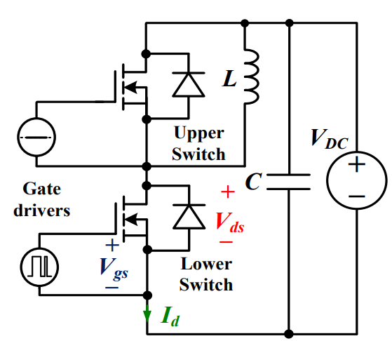
A. Switching Sequence of Cascode GaN/SiC Device: In Figure 2, the Class E inverter's cascode GaN/SiC device exhibits a specific switching sequence. Reducing gate losses can be achieved by adding external capacitors in parallel to the SiC JFET. However, this comes at the cost of an increased maximum drain voltage for the GaN FET. Careful consideration is necessary as it may impact the overall performance and reliability of the system. Balancing these factors is crucial when optimizing the inverter's design for efficiency and robustness.

Fig 2: Switching sequence with hard and soft turn-on time.
B. Analyzing SiC JFET Gate Loss in Cascode GaN/SiC Devices: Gate loss in SiC devices is typically high in HF/VHF circuits due to gate charge and voltage. However, cascode GaN/SiC devices offer zero gate loss in soft-switching with minimal Rg, Jfet. Turn-off charges Coss of GaN FET and SiC JFET capacitors by ID. In a soft-switching scenario, SiC JFET gating loss can be eliminated; in hard-switching, it can be reduced by half. Fig 3 shows the turn-on process of the GaN FET and all of the SiC JFET capacitors.

Fig 3: Cascode GaN/SiC device's turn-on behavior in a Class E inverter schematics.
C. Energy Loss of Small Signal Coss and Large Signal Coss : The small signal Coss of the cascode GaN/SiC device was measured using an impedance analyzer from 0 V to 560 V at 1 MHz. When the DC drain voltage is below -Vth,Jfet, Coss is similar to GaN FET. Above -Vth,Jfet, most voltage is blocked by SiC JFET, making Coss a combination of Coss,Jfet and Coss,GaN. At 500 V, the measured Coss is 40 pF with Vds,GaN ranging from 7 V to 17 V.
Ⅱ. Studying SiC Mosfet, SiC JFET and Cascode GaN/SiC Device in a Class E inverter and their Advantages
The researchers compared a cascode GaN/SiC device and SiC MOSFET and SiC JFET in Class E inverters. The cascode device showcased several advantages over individual SiC devices. Firstly, it exhibited a higher breakdown voltage of 1350 V, providing increased robustness for high-power applications. Secondly, the cascode configuration led to a simpler and smaller auxiliary gate drive circuit since the SiC JFET in the cascode device could draw its gating power from the circuit's main supply. As a result, the gate driver only required driving the GaN FET, reducing complexity and board space requirements. Figure 4 shows the performance of the drain voltage and gate-to-source voltage Vgs(t) of the SiC JFET in the cascode.

Fig 4: Waveform of the drain voltage and gate-to-source voltage in the SiC JFET in the cascode device.
In contrast, using the SiC JFET alone demanded a higher-power gate driver and a separate isolated DC-DC converter was needed to supply the negative gate voltage. The gate drive circuit for the cascode GaN/SiC device proved to be the simplest among the three, requiring less than 1 W from a 5 V gate driver, while the SiC MOSFET and SiC JFET needed 40 W from a 20 V gate driver and 20 W from a -20 V gate driver, respectively. Overall, the cascode GaN/SiC device's advantages in breakdown voltage and gate drive circuit simplicity make it an attractive option for power electronics applications, especially where high-voltage capabilities and efficient gate driver design are essential considerations.
The integration of cascode GaN/SiC power devices offers several advantages over traditional GaN-on-Si devices. SiC has a lower lattice and thermal expansion mismatch with GaN, resulting in smaller Coss losses and higher drain current ratings. Additionally, SiC's higher thermal conductivity facilitates better heat dissipation. Integrating the cascode device reduces parasitics, enables smaller Rds,ON, and minimizes SiC JFET gate power loss. The integration also allows for a reduction in gate resistance by redesigning the device structure and the p+ gate region. These improvements make the cascode GaN/SiC device a promising option for power applications.
Ⅲ. Conclusion
Researchers compared the performance of Class E inverters comprosing of SiC MOSFET, SiC JFET, cascode GaN/SiC device. Cascode achieved highest efficiency, simpler, cheaper, smaller drive circuit. As a future scope integration of cascode GaN/SiC for high-frequency and high-power circuits can be done for further investigation
 Discovering New and Advanced Methodology for Determining the Dynamic Characterization of Wide Bandgap DevicesSaumitra Jagdale15 March 20242471
For a long era, silicon has stood out as the primary material for fabricating electronic devices due to its affordability, moderate efficiency, and performance capabilities. Despite its widespread use, silicon faces several limitations that render it unsuitable for applications involving high power and elevated temperatures. As technological advancements continue and the industry demands enhanced efficiency from devices, these limitations become increasingly vivid. In the quest for electronic devices that are more potent, efficient, and compact, wide bandgap materials are emerging as a dominant player. Their superiority over silicon in crucial aspects such as efficiency, higher junction temperatures, power density, thinner drift regions, and faster switching speeds positions them as the preferred materials for the future of power electronics.
Read More A Comprehensive Guide to FPGA Development BoardsUTMEL11 September 202514711
This comprehensive guide will take you on a journey through the fascinating world of FPGA development boards. We’ll explore what they are, how they differ from microcontrollers, and most importantly, how to choose the perfect board for your needs. Whether you’re a seasoned engineer or a curious hobbyist, prepare to unlock new possibilities in hardware design and accelerate your projects. We’ll cover everything from budget-friendly options to specialized boards for image processing, delve into popular learning paths, and even provide insights into essential software like Vivado. By the end of this article, you’ll have a clear roadmap to navigate the FPGA landscape and make informed decisions for your next groundbreaking endeavor.
Read More Applications of FPGAs in Artificial Intelligence: A Comprehensive GuideUTMEL29 August 20253609
This comprehensive guide explores FPGAs as powerful AI accelerators that offer distinct advantages over traditional GPUs and CPUs. FPGAs provide reconfigurable hardware that can be customized for specific AI workloads, delivering superior energy efficiency, ultra-low latency, and deterministic performance—particularly valuable for edge AI applications. While GPUs excel at parallel processing for training, FPGAs shine in inference tasks through their adaptability and power optimization. The document covers practical implementation challenges, including development complexity and resource constraints, while highlighting solutions like High-Level Synthesis tools and vendor-specific AI development suites from Intel and AMD/Xilinx. Real-world applications span telecommunications, healthcare, autonomous vehicles, and financial services, demonstrating FPGAs' versatility in mission-critical systems requiring real-time processing and minimal power consumption.
Read More 800G Optical Transceivers: The Guide for AI Data CentersUTMEL24 December 20253844
The complete guide to 800G Optical Transceiver standards (QSFP-DD vs. OSFP). Overcome supply shortages and scale your AI data center with Utmel Electronic.
Read More Xilinx FPGAs: From Getting Started to Advanced Application DevelopmentUTMEL09 September 20254301
This guide is your comprehensive roadmap to understanding and mastering the world of Xilinx FPGA technology. From selecting your first board to deploying advanced AI applications, we'll cover everything you need to know to unlock the potential of these remarkable devices. The global FPGA market is on a significant growth trajectory, expected to expand from USD 8.37 billion in 2025 to USD 17.53 billion by 2035. This surge is fueled by the relentless demand for high-performance, adaptable computing in everything from 5G networks and data centers to autonomous vehicles and the Internet of Things (IoT). This guide will walk you through the key concepts, tools, and products in the Xilinx ecosystem, ensuring you're well-equipped to be a part of this technological revolution.
Read More
Subscribe to Utmel !
![ATAES132A-MAHER-T]() ATAES132A-MAHER-T
ATAES132A-MAHER-TMicrochip Technology
![TLE8263EXUMA1]() TLE8263EXUMA1
TLE8263EXUMA1Infineon Technologies
![HCS365/P]() HCS365/P
HCS365/PMicrochip Technology
![HCS200/P]() HCS200/P
HCS200/PMicrochip Technology
![DLPA2005ERSLR]() DLPA2005ERSLR
DLPA2005ERSLRTexas Instruments
![ATSHA204-SH-CZ-T]() ATSHA204-SH-CZ-T
ATSHA204-SH-CZ-TMicrochip Technology
![SN74AVC6T622PWR]() SN74AVC6T622PWR
SN74AVC6T622PWRTexas Instruments
![MOC3061VM]() MOC3061VM
MOC3061VMON Semiconductor
![PAM8904JPR]() PAM8904JPR
PAM8904JPRDiodes Incorporated
![AD9961BCPZRL]() AD9961BCPZRL
AD9961BCPZRLAnalog Devices Inc.


 Product
 Brand
Brand Articles
 Tools
Tools


